Search the Community
Showing results for tags 'fpga'.
-
 Recently I resinstalled LabVIEW 2019 and FPGA19.0 ,FlexRIO 19.0 and I couldnt find where to change the number to compile at the same time. Im pretty sure there is an option in LabVIEW 2019 when trying to comile FPGA VIs ,if you input 3 then three VIs can compile at the same time.(By default you can only compile one ,which is relatively slow when I have multiple VIs which requires many hours each to compile.) Now I just cannot find where to change the number, does anyone there know where and how to change the number? Thanks.
 -
 Hello, I am just trying using Scripting to put Property Node and Method Nodes for accessing a serial port in FPGA VI. I can get these Nodes, and I suppose the property list and method are correct - but I don't know how am I to specify the serial port for these Nodes - when I select the port manually for a Node, it becomes correct. I can get the Property Node with FPGA I/O terminals (till npow I did not try this with a Method Node), but I don't know what should I put into a constant that I will connect to FPGA I/O input terminal (when I added the constant manually there, I was unable to select a serial port from I/O items menu). I can also use the Scripting to find serial ports in the target where I am putting the edited VI (it has Type String "RIO Subresource", Name "Port1", and Item ID (non-0, while its Source ID contains 0-s only). I am creating these Nodes using EIOPlaceDownEIOPropertyNode.vi and EIOPlaceDownEIOMethodNode.vi; the State input contains item="Mod1\Port1", the name is shown in the Node header line, and it is the same after assigning the serial port manually, but the manual assignment is needed to get the port name recognized. Have anyone found what function and how can be used to specify a serial port for these Nodes? Thanks in advance for any hint, Jerzy Tarasiuk
 -
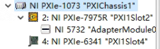
I have a PXIe-7975R(FlexRIO FPGA with 5732 digitizer)and a PXIe-6341(DAQ) both installed in a PXIe-1073 chassis(you can check in screenshot below) and I want to synchronize there two device. my goal :The DAQ will output some control signal and the FPGA will acquire some other signal and they are synchronized . what I tried: 1. output a digital signal to 5732, however its DIO port somehow dont work,and that force me to input signal using AI port,but there are much much noise 2.this chassis used to run ScanImage( https://docs.scanimage.org/ an program based on MATLAB using DAQmx API),so Im sure the same thing could be realised using LabVIEW,however I couldnt find a way to do so. So ,is there a way to synchronize there two device?Or are there some modules like DAQmx avalible?(examples of 5732 only demonstrates Clock Select and Streaming)

-
... to provide us with an upgrade to our software which we bought back in 2017. And this is going on for more than a year now. The story is simple - our company bought a license for NI EMBEDDED CONTROL AND MONITORING SOFTWARE SUITE, USB, SPR17, Rev 007, 2017.06.07 and we successfully downloaded the SP1 upgrade later on. The next year we bought a subscription to LabView 2018 but did not renew it for 2019 and went back to using 2017. Meanwhile our downloaded SP1 files gone missing. "No problem" - we thought - "We'll just go to the NI website and download our SP1." https://www.ni.com/en-ca/support/downloads/software-products/download.embedded-control-and-monitoring-software-suite.html#306390 Not that fast! To download previous versions of LabView you need an active subscription. OK... So, how do you get missing pieces for your software you have a license for if you do not have an active subscription? We contacted NI and their representative Newark and asked them for help... Long story short - we are still waiting for a resolution. Meanwhile, I see no other option but to ask the community for help if NI is so ignorant. Maybe some of the members can share their LabView 2017 SP1 installation files? I don't think it will be a copyright violation or something - what can you do with it without the license? In any case, I would greatly appreciate any input and, maybe, perhaps an advise or a comment. https://www.ni.com/en-ca/shop/software/products/embedded-control-and-monitoring-software-suite.html We are looking for: 1. LabView2017SP1-WinEng 2. 2017SP1RealTime-WinEng 3. 2017SP1FPGAModule-WinEng 4. 2017SP1XILINXCompilationTools Best Regards.
-
Hi, So I have question about the inner working of the host to target FIFO for a setup with a Windows PC and a PXIe-7820R (if the specific hardware is important). But it really isn't so much of question as me trying to understand something. My setup: I transfer data from host to the target (the FPGA module 7820). First I simply configured my FIFO to use U8 as datatype and read one element at a time on the FPGA target. It worked but when I increased the amount of data I ran into a performance issue. In order to increase the throughput I both increased the width of the FIFO, packing four bytes into one U32, and also reconfigured the target to read two elements at a time. This worked, so there really isn't any issue here that needs to be resolved. But afterwards I thought occurd: would I have achieved the same result if I kept the width U8 but read eight elements at a time on the FPGA? Since 4*2 and 1*8 both are 8, would I have achieved the same throughput? Or is it better to read fewer but longer integers (and then splitting them up into U8's)? I've read NI's white paper but it doesn't cover this specific subject. Thanks for any thoughts given on the topic! 😊
-
Hi guys. This semester I'm starting a course system development for control and automation engineering, witch will be based on LabView. Therefore, my University doesn't have a NI hardware, even a MyRIO for us to test our VI and the teacher said that we should test our projects with our own Arduino... So, I have a little experience in Arduino and I know the basics for LabView. Now I'm in a point that I know that with Arduino I'll not take the best from LabView. I cannot even deploy a code to it. So, there is where my question comes in... I'm looking for a new board better then Arduino to use in the classes. I would buy a MyRIO card if I had the money but in Brazil this board is too expensive for me Witch one should I get that is closest to myRIO and less expensive than that? I would like to try de deployment of a VI and FPGA..... Is this possible? Thanks a lot for the help! Regards
-
Hello. I need change some code for SbRIO-9626 with LabVIEW 2018. I have code from LabVIEW 2015. Right now I have only LabVIEW 2018. And I worked with it for SbRIO-9627. LabVIEW FPGA, LabVIEW Real-Time, NICRIO1800 driver istalled. And I install Xilinx ISE 11.5 Compilation Tool too. When I start compilation FPGA VI I got error about problem with compilation too (see attachment picture). Could you tell me how I can solve this problem? It is very important.
-
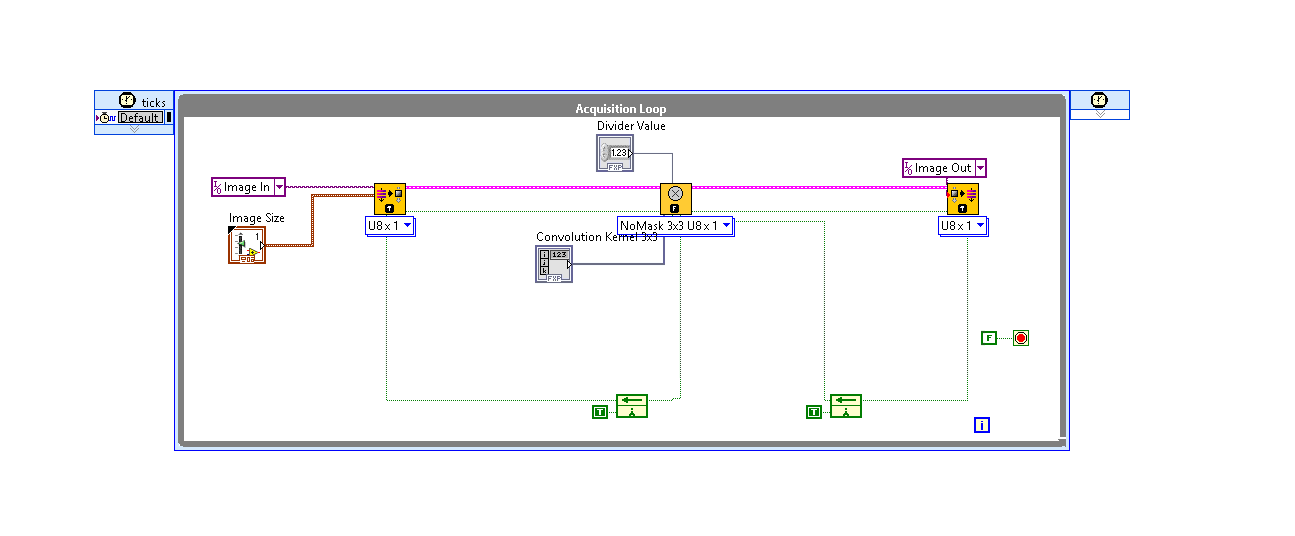
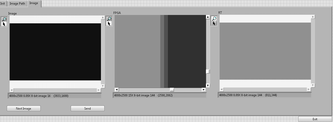
Hi, I am trying to use image convolution inside FPGA. My Image size is around 6kx2k. The convolution is applied properly until 2600 pixels in x resolution. After that, the values seem to miss previous row data. In Detail: As convolution is matrix operation, image data needs to be stored for the operation. But it seems there is an inadvertent error storing only 2600 pixels per row inside FPGA. And hence the filtered output is calculated assuming these pixels to be 0. I have tried with different image sizes, different convolution kernels, and also in different targets (cRIO 9030 and IC 3173). All results are same. I have attached a screenshot of FPGA VI and an example image. The example image shows an input image of 4000x2500 of same pixel value 16.The kernel is 3x3 of values 1 with divider=1. The RT image is processed using IMAQ convolute inside RT controller and has value 144 [(9*16)/1] for all pixels. But the FPGA processed image (zoomed in) has 144 until 2597 pixels and then 112 (7*16- showing 1 column of 2 rows missing) at 2598, 80 (5*16- showing 2 columns of 2 rows missing) at 2599 and 48 after that (missing 3 columns of 2 rows- current row is always present). This shows the data is missing from the previous rows after 2600 index. Is there some mistake in the code or any workaround available?
-
Hi, If I generate an FPGA IP core from my LabVIEW code, can I use it somehow in traditional FPGA development environments, such as Vivado? Thanks, David
-
Hello everyone, I’m not sure which forum is the right one which is why I created two new topics with the same content (one in Embedded and one in VI Scripting) – so sorry for the spamming. I have two questions: How can I generate a cRIO project programmatically? How can I start the “Discovering Devices” tool of the Project Wizard automatically? At first I will describe a bit more what I really want to do: I’m about to write an auto coder which should create a complete new FPGA project on my cRIO system without any user input. In the Project Wizard I want to run the “System Setup” from NI standalone. In that mask the NI project need some input like project type which is always a cRIO Embedded System. The next step is to insert an IP address to discover an existing system. As those two steps are every time with the same input, I want to give them those parameters so that everything runs automatically. Is there anybody who can help? Thanks a lot!!
-
Hello everybody, I'm about to write an application that can create a complete new FPGA-Project for the cRIO-system automatically without any user Input. Before I ask my question directly, I will give you a few Information about the system and how it works at the moment. I'm working with a cRIO-system that can have different modules in different slots (max 8). That system should be universally usable which means I can replace one module with another one at the start up and create a complete new project with a different name. Most of the project works (I can find out in which slots which module is placed and load the right VI's correctly) but there is one point which I really dislike: the user always has to give some input Information at the beginning of the creation and mostly that is the same like "Which type of project it should be" or "Which IP address should be used to find the system and the modules for each slot". The goal is that I can write down some specific arguments so the program is created automatically? Or - if there is no way to do this - a way that a second window is shown on screen to help the user through the creation process (for example that tells the user that the system need to be turned on that the project can find every single module)? English isn't my mother tongue, so please apologize if there are any mistakes in my spelling. Thank you very much for your help
-
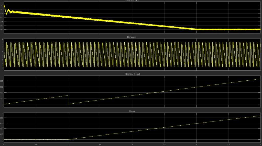
 Hello, everyone. Recently I came across one issue, that I solved within a couple of minutes in Simulink, but cannot crack for a couple of days in LabVIEW. It is a Rising integrator (model and plots from Simulink attached). Mod is the modulus function (i.e. remainder), the integrator reset is triggered by the external “Trigger” signal at 1 sec. After that, as you see the integrator generates a ramp signal. I was trying to represent the same behavior in FPGA LabVIEW in order to use it further on my cRIO. I’ve seen on the forum, that one of the most feasible solutions for the Quotient & Remainder function (i.e., Modulus in Simulink) is the use of a while loop system with subtraction. But the behavior of the system is different since it generates a ramp signal after the reset is on, but it has a negative slope and saturates at -37k. Just to check in general how the approach works in LabVIEW, I’ve designed the second model with a Quotient & Remainder block (I know that for FPGA it is not the best option, plus I could not figure but how to use it with FXP values). But this model generates the output with a value of 5. Which is even more questionable. In this case, could you please advise what I am doing wrong with the FPGA code for the block? Since FPGA is the main reason, why I am looking for any options but not to use the Quotient & Remainder block. Thank you in advance. P.S. The models are designed in LabVIEW 2014 SP1. Integrator_SGL.vi Integrator_while_loop.vi
-
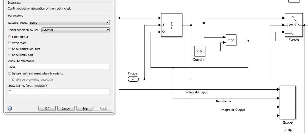
Hi all, working on my first reconfigurable IO project using a PXI 7811R with LabVIEW RT. I am building a quadrature encoder counter using a couple of the NI examples, and was wondering if there were any caveats to changing it to use an I-64 as the counter output? The NI example uses a 32 bit integer for the count. In my version, I changed it to an I64 count output and added a speed (counting ticks between pulses) output as well. It seems to work fine, but would appreciate any cautions that experienced FPGA users might have. Neville. PS. Cross posted to info-LabVIEW as well.
-
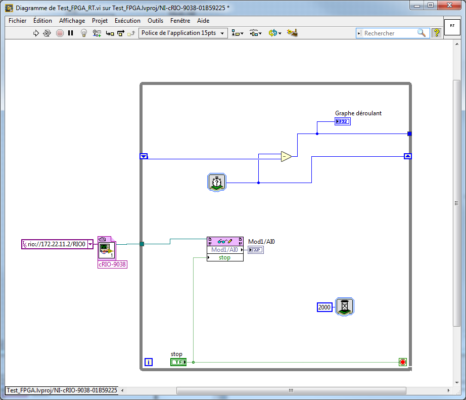
Hello, I'm currently encountering a problem when accessing FPGA indicator with "Reading/ writing a control" node The FPGA part acquires data every 10µs The RT part Read the indicator every 2000µs But when Running the VIs, I see that the elapsed time between 2 Readings of the indicator change from one iteration to another Can someone help me?
-
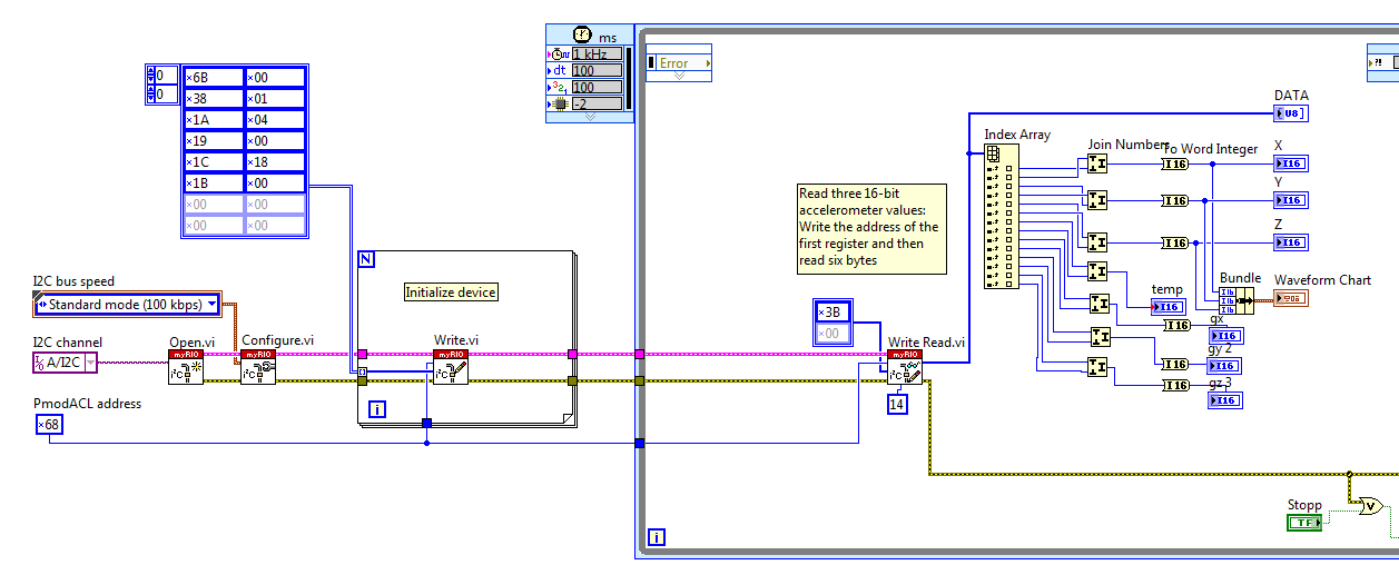
Hi Folks, The scenario is, I have a sbRIO 9651 and a MPU 6050 (A IMU sensor). I would like to acquire sensor data in FPGA VI, stream it to RT VI for processing and analysis and view it from windows based VI. I came across certain problems which I wasn't able to figure out. I dont have the appropriate cable to interface the sensor yet, which I have ordered, to test the VI. 1. FPGA VI: The I2C Master VI outputs a array of 14 bytes raw data (6 bytes for Accelerometer, 6 bytes for gyroscope and 2 bytes for temperature). since the data can only be written element by element in a DMA FIFO, how can I stream an array to RT VI. I did an auto-indexed for loop to write data but I dont know if this will work. 2. RT VI: Initialization of MPU6050 is done here. It involves writing a byte array sequence to I2C Master VI to configure it and then a write-read(writing a register to read data from) process to acquire data. I am not sure how to do the write- read part. I was able to do it in myRIO RT Vi as it had clear APIs 3. The single process shared variable 'RT Stop' used for communication between loops in RT VI is written a value after the loop ends which I dont know as to why. The architecture is based on the Turbine example from cRIO developers guide. I am attaching the VIs for your reference. Please have a look into the code and let me know if you find anything that needs correction. I am totally new to Real time and FPGA programming. Thanks a ton Gokul first1.lvproj RT VI.vi FPGA acq.vi first1.lvproj
-
My setup is: - PXIe-1082 chasis - PXIe-7962R FlexRIO - custom MRF timing card I want to send data via the DStarB line from the custom FPGA to the FlexRIO. I am reading the DStarB line in my LV FPGA program. The problem I have is that I only get the data when the DStarB line goes from '0' to '1'. If I send two '1' after another I only get the first one, because I only recognize the positive front. I would wager that the backplane has a setting for this DStar lines. Some pull-downs or something... I cannot read the VI_ATTR_PXI_DSTAR_BUS and VI_ATTR_PXI_DSTAR_BUS_SET attributes of the PXIe-7962 card from the LabVIEW program. The attributes are also not present in the VISA Interactive control Attributes list. Is there a problem, because the crate is not configured to work with my custom timing card? Or is the problem in the FlexRIO configuration? Do I need to enable something in the chassis settings in NI MAX? I went over everything but cannot find something useful. Do I need to configure the backplane with my timing card somehow? I am running out of ideas, so please do help.
-
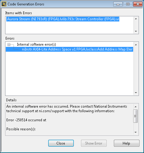
I'm at a loss for what could be happening so I'm hoping somebody else has done something similar. I am using LabVIEW 2015 SP1 with the FlexRIO 15.5 drivers with the 7935R and receive an internal software error when trying to compile the example project "NI793xR - MGT Aurora CLIP.lvproj" when generating intermediate files. The Error I'm getting is copied below. Error -250514 occurred at Possible reason(s): An AXI4-Lite address map element cannot fit in the specified address collection. Make sure that each address map elements' offset plus size does not exceed the address collection's total size. My goal is to replace the DRAM FIFO that is currently being used to write to Port 0 with a Count Up, Count Down, or PRBS signal. I was receiving the same compilation error after trying to make these changes. I tried to be very careful with what I replaced and was pretty confident that I hadn't touched any of the AXI4 functions. I tried compiling the example project because I was going to start over and make sure I had a good starting point. The example does run but that's using the bitfile that's already compiled. I've tried compiling using the cloud as well as a company compile server. I'm also installing software so I can try this on another computer. I don't think I need the tools locally for this but I might try installing those to double check. Pretty much out of ideas and wasn't able to find much online so any help would be appreciated. Matt J Edit: Same compilation error on second computer with local tools, both Windows 7.
-
Hi, I am quite familiar with different design pattern on LabVIEW but I am a newbie on FPGA design. I start working on a project for my own hobby using myRIO to control motor speed with PWM and read back encoder. This is the first part of my project and I plan to expand more later. This project will help me to get use to FPGA too. I am trying to learn a good design pattern by follow the template project which is "LabVIEW FPGA control on Compact RIO". In this template project, feedback value and control signal are analog channels and they connect directly with PID module in FPGA in a normal while loop. The configuration are sent from host. In my prototype project, I already built FPGA module to drive PWM and read encoder using single-cycle time loop. I plan to use PID in real time code. If I want to follow the template design, I have to change the way I implement the code for FPGA and Real-Time. So right now, I am not sure what is a good design I should follow. If you have any advice, I will highly appreciate. Thank you very much!
-
Hey guys, I'm trying to do some scripting on a Realtime-VI wich uses the FPGA Interface "Read/Write Control". I open a Reference to a VI containing a Read/Write Control, and when scrolling through the BD-Objects I find it with the class-name "nirviReadWriteControl". I used the "to more specific class"-VI to check wich class i can cast it to, and i tracked it down to be child of the GObject->Node Class. But i can't cast it to any of the childs offered in the class specifier constant. I also found out, that the "nirviReadWriteControl" is a xnode. I have never worked with those, is there a way to access theyr methods (I think they're called "abilities" for xnodes)? The goal of the application is to make the Read/Write Control display all available FPGA FP-Elements, and connect Controls/Indicators to them. There is the same Problem with the "Open FPGA Reference"-Node (Classname "nirviOpenFPGA"). I really hope somebody dealed with the xnodes a bit and can help me programmatically controlling them! Best, Trip
-
Hi FPGA expert. When I try “my way†of implementing a simple FPGA Analog Out VI, I run out of FPGA fabric (too may LUTs used). So what better way can I do this (if there is one), that don’t overuse my LUTs. My task is to: Make one analog measurement and control 2 analogue outputs that should be clocked out every time I get a digital trigger in. I’m running a sbRIO-9637 (Zynq7020) I’ve attached the simple application and I’m puzzled of what needs so many Look Up Tables (LUTs). Any suggestions? FPGATest.zip
-
I have a system that composed of 1- NI-cRIO9014 2- Chassis (cRIO-9104) 3- Three Mods. NI9215 I use this system to capture 12 analog signals. What is the relation between sampling frequency defined by time delay in fpga.vi and the Requested number of Elements defined in FIFO?. When I use a time delay of 40us and Requested number of Elements 8191, it produces wrong data. When I use a time delay of 40us and Requested number of Elements 65535, it produces correct data.
-
Hello all, a new control board based on the NI System on Module, formally sbRIO-9651, has been developed by an Italy based company. It is mainly devoted to industrial control as well as power electronics and drive applications. Each peripheral is supported by dedicated LabVIEW drivers as well as by demo projects... www.ped-board.com (UPDATE) Adapter Boards have been released for industrial and power electronics and drives applications: http://www.ped-board.com/adapter-boards/ Cheers, sirb
-
I have a system that composed of 1- NI-cRIO9014 2- Chassis (cRIO-9104) 3- Three Mods. NI9215 The following are properties of my current FPGA Target Class: cRIO-9104 FPGA Device Information: Family: Virtex-II Type: xc2v3000 Speed Grade: -4 Package: fg676 Compiler Information: Version: Xilinx 10.1 Xilinx Options in Build Specifications: Supported Host Computer/FPGA Communication: Programmatic FPGA Interface Communication: Supported Interactive Front Panel Communication: Supported Number of Logical Interrupts: 32 DMA: Number of DMA Channels: 3 Multi-Element Access on Target: Not supported Peer-to-Peer Streaming: Not supported Type: Target to Host - DMA Control logic: Slice Fabric I am reading 12 Analog signals, I do not know what is the maximum value for Requested Number of Elements I can use? The General page help says a size of 2^M-1, What is M?
-
Still learning about the cRIO, but thought I'd share some of what I've learned recently. Some background on what was going on... We had a driveline failure on two test stands out at customer site. There are sheer pins in the driveline designed to fail rather than send massive torque through a gear set in ways that is just BAD as it can lead to dynamic testing of the hard guarding (which is always fun!). Long story short, there was a failure more of the sheer pins that required detection of the sheer pins breaking. Worst case conditions is the break occurs at 6000 RPM and the only thing that we have already in the system is a 1 mm wide match mark on a 25 mm diameter disk. We found some laser sensors that could pick up the mark and bench tested the system. Everything looked good, so we integrated the bench test in the project, compiled everything and went to update the cRIO. This involved adding C series modules (electrician on site) and remote update of the cRIO application and bitfile through TeamViewer. Lessons learned... 1. Install the NI-RIO driver on a PC connected to the cRIO before it is 1000s of km away. Transferring 4GB of installer over a flakey TeamViewer connection is not recommended. 2. Replication and Deployment (RAD) utility works well for the RT portion, but may not be able to install a bitfile to the FPGA. 3. The example "Get & Set Real-Time System Image" can work when RAD does not. Building the example into an executable that can deploy a selected file is very useful. 4. It is possible to create a image using RAD without errors from an identical cRIO that does not have all of the C series modules. There will not be an error, however the image will not deploy/set (sometimes without an error message). 5. Shared variables can function correctly with different LabVIEW versions (person helping me accidentally converted everything to 2015 for the image that did eventually install). I'm sure I'm missing something, so would appreciate any insight people have.